







 发布时间:2026-09-22
  浏览量:0
浏览量:0  文章来源:
文章来源: The challenges and innovations of massive transfer repair technology?
What is the overall efficiency of massive transfer detection and repair?
This article will make it clear to you at a glance!
1. What are the challenges of inevitable defect repair in massive transfer?
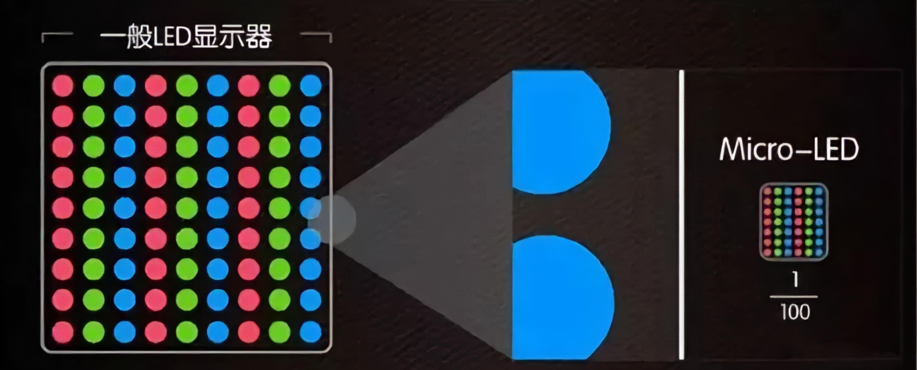
Micro LED pixel integration is different from OLED in that it does not use organic vapor deposition to achieve the integration of light-emitting units, but instead uses a massive transfer method to bond hundreds of thousands of micro level LED chips onto the driver backplane. Due to the large quantity, small chip size, and high precision requirements, Micro LED displays inevitably introduce defects in the LED chip process and LED and backplane integration process. Therefore, repair has become a necessary process in the manufacturing of Micro LED screens. The factors that affect the Micro LED repair process mainly include the yield, efficiency, and cost of the repair. In terms of yield, due to the small size of Micro LED chips, with lateral dimensions ranging from tens to even a few micrometers and thicknesses below 10 μ m, and the differences in repair processes caused by the different materials of R-LED and GB-LED, it is a challenging task to effectively remove and repair bad chips after identifying them. In terms of efficiency, taking 4K products as an example, if the number of LEDs on the screen exceeds 24 million, and the transfer yield is 99.99%, then the number of bad pixels that need to be repaired reaches 2400. Therefore, if Micro LEDs are industrialized, the repair efficiency must be guaranteed on the premise of a reliable repair success rate. In terms of cost, in addition to the impact of yield and efficiency on costs, the cost of repair materials and BOM is also an important consideration factor. It is necessary to reduce repair costs while ensuring the success rate of repairs.

2. How can Chenxian Optoelectronics achieve efficient repair and reduce losses?
Chenxian Optoelectronics combines two solutions, namely massive repair and single repair, to accurately calculate the input-output ratio of massive repair and single repair, and determine whether to use massive repair or single repair at each site. Simultaneously developing more cost-effective repair solutions to reduce repair costs while improving repair yield.

3. How can Chenxian Optoelectronics' innovative practice improve the overall efficiency of detection and repair?
Chenxian Optoelectronics reduces the repair workload of difficult repair sites by optimizing the process flow. Secondly, collaborate with upstream manufacturers to develop high-precision detection and repair equipment, especially to enhance algorithms and data acquisition hardware, in order to provide more accurate repair coordinates. In addition, we also collaborate with repair material manufacturers to develop high yield and high reliability repair materials, ensuring repair quality while improving overall efficiency.