







 发布时间:2026-06-29
  浏览量:3
浏览量:3  文章来源:
文章来源: The Necessity and Challenges of Massive Transfer Detection?
The process and equipment for massive transfer detection?
This article will make it clear to you at a glance!
Why is the detection of massive transfers a critical step?
Large scale transfer detection is a key step in ensuring the quality of the screen, aimed at identifying and accurately locating bad pixels in the process, and then outputting these coordinates to the repair process to improve the lighting yield and image quality of the screen. At present, the detection methods mainly include visual inspection, optical inspection, and electrical inspection, which are carried out at the wafer end, process end, and screen end respectively, to achieve accurate detection of process defects. In addition, to address the issue of insufficient optical uniformity in Micro LED chips, Chenxian Optoelectronics has adopted mixed bin technology to accurately classify Micro LED incoming materials through optical and electrical detection, thereby improving display performance.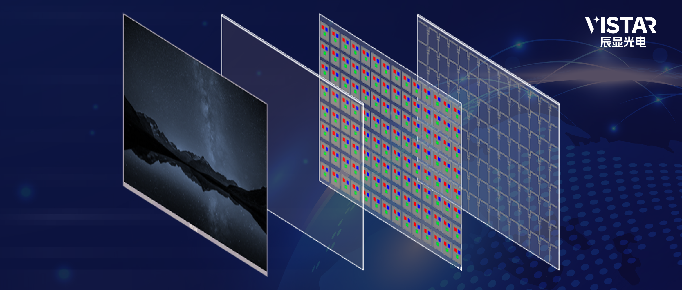
What are the main challenges currently faced by the industry in large-scale transfer detection?
-
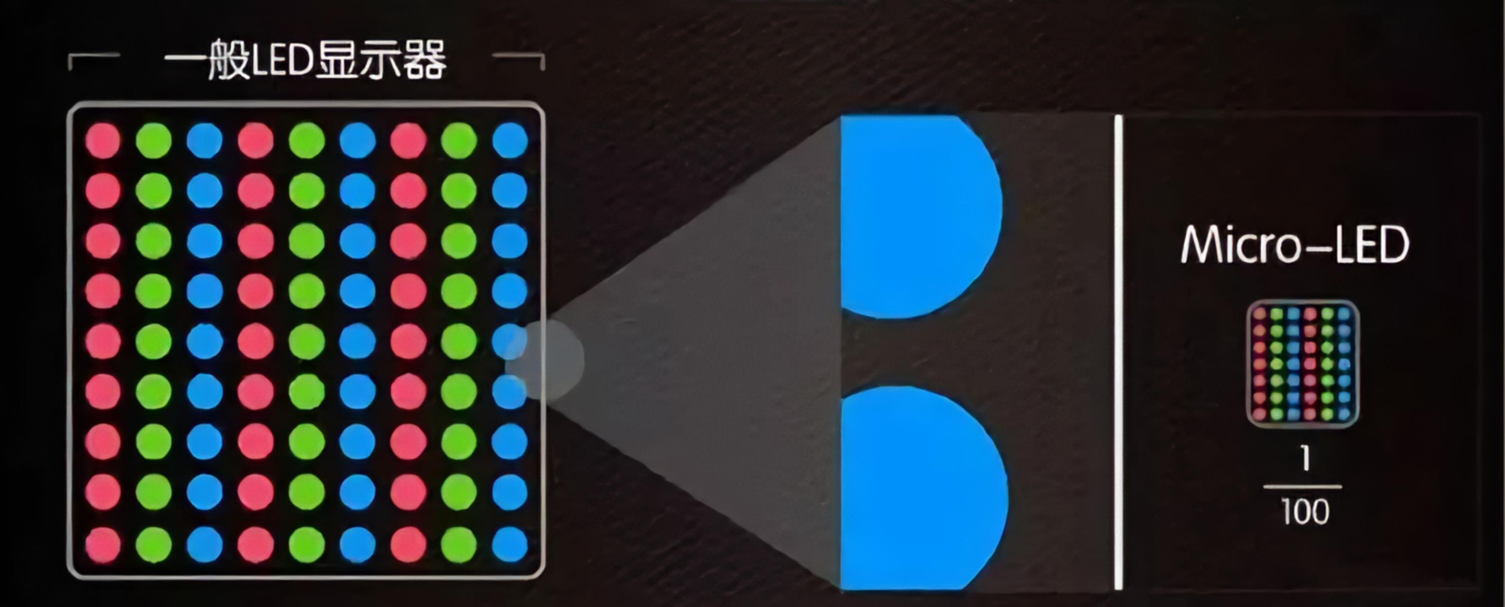
With the miniaturization of Micro LED chips, traditional detection methods and equipment are unable to meet the demand. Firstly, the challenge faced by electrical testing is that each display needs to detect tens of thousands or even tens of millions of LEDs. Due to the limitation that Micro LED chips are generally less than 50 μ m, the current detection efficiency is still in the stage of 1-2 seconds and cannot meet the requirements of full LED inspection. Secondly, the detection accuracy requirements are extremely high. In the Micro LED process, the precision requirement is generally within 2 μ m, and high PPI products even require precision within 1 μ m. This places extremely high demands on the precision detection of Micro LED chips at every stage from the wafer to the intermediate temporary substrate and back panel, which must be achieved through the combination of intelligent algorithms and high-precision data acquisition hardware.

-
How to build an efficient large-scale transfer detection process for Chenxian Optoelectronics?
Chenxian Optoelectronics has deployed multiple detection stations in the large-scale transfer process to improve the yield and precision repair capability of the first transfer. Firstly, Micro LED wafers undergo appearance (AOI), optical (PL), and electrical (EL) inspections upon receipt to ensure the yield and photoelectric information of Micro LED materials, and to centrally repair defective points. In the transfer process, adverse factors such as missing or offset are identified through AOI detection and repaired in a timely manner. Finally, perform CT inspection on the screen after bonding to check the optical quality of the screen, including bright and dark spots, abnormal display, brightness and wavelength consistency, etc., and output the coordinates of the detected defect points to the next site for repair. Through layer by layer inspection and repair, Chenxian Optoelectronics is able to produce high-quality, zero dark spot screens.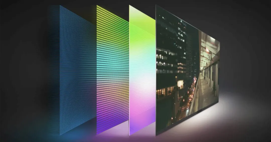
What are the first domestic devices or technologies used by Chenxian Optoelectronics for testing?
-
Chenxian Optoelectronics attaches great importance to close cooperation with domestic equipment manufacturers. In the early stages of Micro LED industrialization, it introduced multiple advanced domestic technologies and equipment, especially in the field of detection, covering key detection links such as AOI, PL, CT, etc., to ensure the efficiency and accuracy of the detection process. As Micro LED is an emerging technology, with the continuous improvement of technology and process requirements, Chenxian Optoelectronics and equipment manufacturers have jointly promoted the iteration of equipment and technology, and cooperated to develop multiple domestic first sets of equipment, further promoting the industrialization process of Micro LED.
-